Key Takeaways
This analysis of Huawei’s first-generation Ascend 910 series (2019) and second-generation Ascend 910B series (2022) suggests that despite facing export controls, Huawei was able to design a higher-performing chip that could be manufactured domestically at SMIC and meet some of China’s domestic demand for AI compute. Nonetheless, our analysis reveals that the performance increase is smaller than advertised; only 75 percent of the theoretical maximum performance increase can be attributed to an actual increase in hardware performance. Additionally, Huawei reduced the number of active AI cores between the 910 and 910B series—likely either due to poor yields or limited capacity on SMIC’s 7nm fabrication process.
- Officially, Huawei’s second-generation Ascend 910B series chips have increased maximum theoretical performance by 80 TFLOPS (FP16) compared to its first-generation Ascend 910 series chips. Most 910B models also have faster and more memory capacity. The 910B chips also have fewer AI cores, but each core houses an additional vector unit—moderately increasing the throughput per core.
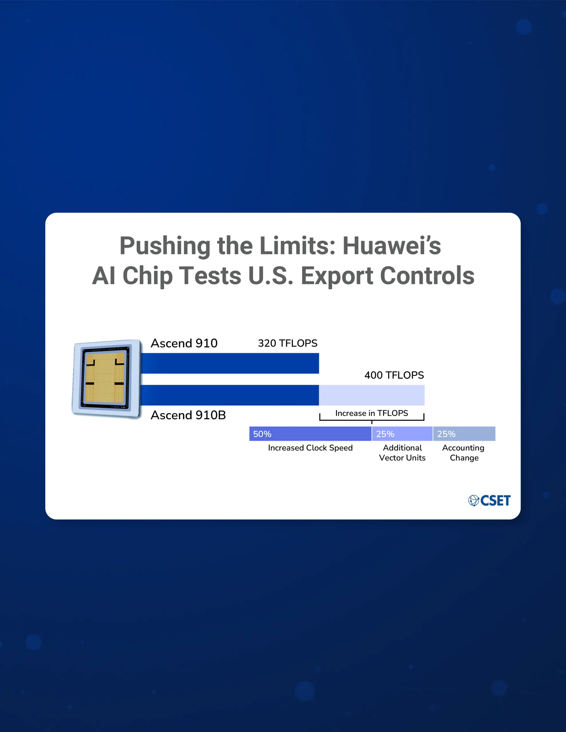
- The performance increase comes from three factors. 50% of the increase is due to an increased clock speed. An additional 25% can be attributed to the additional vector unit in each AI core. And the remaining 25% of the performance increase between the two generations of chips appears to result from a change in how Huawei calculates peak performance.
- Limitations in yield or capacity are likely why the second generation has fewer AI cores. The AI core architecture used in both series appears to be very similar, suggesting that Huawei either a) used a similar-sized die and chip layout, but due to low yields could only activate fewer AI cores or b) used a smaller die that fit fewer AI cores to allow Huawei to fabricate more chips per wafer using SMIC’s limited 7nm fabrication capacity.
While Huawei’s development is significant and demonstrates China’s progress in chip design and manufacturing, U.S. export controls have almost certainly slowed Huawei’s progress.
- Huawei needed at least two years to redesign and domestically fabricate the second-generation Ascend 910B chips, with only marginal improvements. Meanwhile, leading U.S. AI chip design companies designed and produced new chips capable of performance that surpasses any Huawei Ascend chip.
Introduction
Over the last two years, the United States implemented export controls on the chips needed to develop and deploy the most advanced AI systems, seeking to deny China access to those chips. As U.S. policymakers evaluate the policy’s effectiveness, an important indicator to monitor is China’s domestic AI chip design and manufacturing progress.
To provide insight into China’s AI chip design progress, CSET is tracking over 180 AI chip products designed by over 30 Chinese organizations. Of particular interest is Huawei’s AI chip development. Despite being Entity-listed since 2020, Huawei brought AI chips to market that are comparable to one of NVIDIA’s higher performing chips—the A100. In fact, Huawei’s Ascend chips are some of the most advanced Chinese AI chips and are likely the most widely deployed.1
In this data snapshot, we provide insights into how Huawei has been able to domestically design and manufacture AI chips despite U.S. export controls, including what challenges Huawei likely faced and how it worked around limitations.
Background
In 2019, Huawei released its top-of-the-line Ascend 910 chips fabricated on TSMC’s 7nm process node. The chip quickly gained traction in China; it was installed in data centers affiliated with the Chinese government and incorporated into numerous server products.2 But Huawei was forced to halt production with TSMC in 2020 when the Bureau of Industry and Security (BIS) at the U.S. Department of Commerce placed Huawei on the Entity List and imposed the Foreign Direct Product Rule (FDPR) on the company. This extraterritorial control effectively prohibited foreign foundries from manufacturing Huawei’s chips, kneecapping Huawei’s ability to produce its Ascend 910 chips.
Two years later, Huawei began selling a second generation of Ascend 910 chips—called the Ascend 910B series—which are fabricated domestically in mainland China.3 Due to Huawei’s close collaboration with Semiconductor Manufacturing International Corporation (SMIC), these chips appear to be among the select few to use China’s most advanced but highly limited 7nm fabrication capacity.
Ascend 910B: New and Improved
Comparing the two generations of Ascend 910 chips provides insights into how Huawei is designing and manufacturing around U.S. export controls, in particular the FDPR, to supply the Chinese market with high-performance AI chips.4 To inform this analysis, we reviewed technical documentation for both generations of Ascend 910 chips and technical documentation for over 20 server products that incorporate those chips.
While both generations of the Ascend 910 chips are similarly designed, a few key differences are worth noting. The second-generation Ascend 910B chips have higher maximum performance, a higher clock speed but fewer active AI cores, one additional vector unit in each AI core, and a newer memory type with higher bandwidth and capacity.
Huawei created five models of the first-generation Ascend 910 chip, the highest performing of which appears to be capable of 320 FP16 TFLOPS. To put this in context, this is roughly comparable to NVIDIA’s A100, which was state-of-the-art in 2020.5 Ascend 910 models range from 30-32 active AI cores. Each AI core contains one matrix execution unit and one vector execution unit; both types of units are needed to train AI models, but most of the core’s performance comes from the matrix unit, which is specially designed for AI operations.
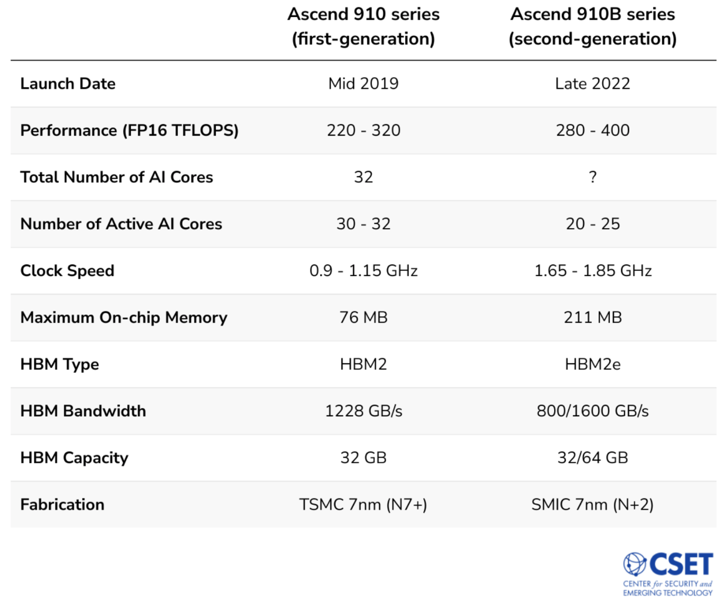
The second-generation 910B series, likely released in 2022, has at least four models. The highest performing of these four models appears to be capable of 400 FP16 TFLOPS. All four models have fewer active AI cores, ranging from 20-25. A key difference between the two generations is that each AI core of the second generation contains one matrix execution unit and two vector execution units—one more vector unit than the previous generation. Huawei likely added a second vector unit because the sole vector unit may have had insufficient throughput, becoming a bottleneck for the matrix unit.6 With an additional vector unit the second-generation Ascend 910B likely can more quickly perform vector operations, which may increase overall AI training and speed. Additionally, compared with the first-generation series, the 910B has twice as much on-chip memory, which should relieve memory bottlenecks and help the chip’s actual performance approach its theoretical maximum. The 910B also features a newer external memory type (HBM2e) with higher bandwidth and double the maximum memory capacity. See Table 1 for a direct comparison between the first- and second-generation Ascend 910 chips.
Huawei also created the Ascend 910C series, which likely was intended to double the performance of the 910B series by doubling the number of active AI cores. However, potentially due to manufacturing issues, Huawei ultimately reduced the specifications for the 910C series to match those of the 910B.7
Table 1: Key Specifications for First- and Second-Generation Ascend 910 Series Chips8

Performance Upgrade: Smaller than it Appears
The increase in theoretical maximum performance from the first-generation Ascend 910 (320 TFLOPS) to the second-generation Ascend 910B (400 TFLOPS) is a significant upgrade. However, a deeper analysis reveals that the performance difference between the first- and second-generation chips is lower than it appears.
In general, a chip’s performance is calculated by multiplying the clock speed (i.e., the number of cycles a chip can perform per second) and the throughput of the chip (i.e., the number of operations a chip can perform per cycle).
Based on CSET analysis, there are three factors responsible for the 80 TFLOPS increase in theoretical performance from the first-generation to the second-generation Ascend 910B chips. Half of the increase (40 TFLOPS) comes as a result of the second-generation Ascend 910B being clocked at a higher speed. Increasing the clock speed means that a chip is able to cycle more times per second, which increases the speed of operation and leads to overall higher performance. Per cycle, the two generations have nearly identical throughput aside from an additional vector unit per core and an accounting change, which are responsible for the remaining increase in performance. More specifically, about a fourth (20 TFLOPS) of the increase can be attributed to the additional vector unit per core incorporated in the 910B. The remaining fourth (20 TFLOPS) comes as a result of an accounting change in how Huawei calculated the chips’ performance.
Figure 1. Factors Responsible for the Increase in TFLOPS Between Ascend 910 and Ascend 910B9

Between the first- and second-generation Ascend 910 chips, Huawei changed which operations it counted towards performance. Even though the first generation appears able to run matrix and vector operations in parallel, Huawei only counted operations performed by matrix units towards the chip’s peak performance—excluding operations performed by the vector units.10 For the second generation, however, Huawei counted operations from both the matrix and vector units.
If we applied the same accounting method to the first-generation Ascend 910 chip (i.e., counting both matrix and vector units towards performance), it would have a maximum theoretical performance of 340 TFLOPS. As a result, the real improvement in maximum theoretical performance is only 60 TFLOPS rather than 80 TFLOPS.
Manufacturing Limitations
As explained above, the second-generation 910B series uses significantly fewer active AI cores than the first-generation 910 series, suggesting yield or capacity constraints on SMIC’s manufacturing process. There are two likely reasons why the second-generation 910B has fewer AI cores. The first possibility is that both generations use 32 total AI cores, but because the yields of SMIC’s 7nm process are low, only 20-25 cores could be activated per 910B series chip. The second possibility is that Huawei made a die with fewer total AI cores, allowing Huawei to fabricate more chips per wafer using SMIC’s limited 7nm fabrication capacity. This could also be an effort to offset the likely die area increase resulting from adding more on-chip memory to the chip.11
Whether due to SMIC’s poor yields or limited capacity, Huawei reduced the number of active AI cores between the 910 and 910B—successfully designing a chip that could be manufactured domestically at SMIC and supplied to the Chinese market. But to accomplish this, Huawei needed at least two years—from when the FDPR was applied in 2020 to when the 910B series first appeared in technical documentation in 2022—to redesign and domestically fabricate the chip. Meanwhile, since 2020, leading U.S. AI chip design companies designed and produced new chips capable of performance that surpasses any Huawei Ascend chip.12
Conclusion
Huawei’s Ascend 910 and 910B chips are both consequential innovations. The first-generation 910 demonstrated that Huawei was a fast follower in AI chip design; Huawei unveiled the 910 before NVIDIA’s A100—claiming similar performance on paper but falling short in practice. Then, in 2022, despite extraterritorial U.S. export controls, Huawei produced the second-generation Ascend 910B chip with improved performance and memory—a true Chinese-made alternative to NVIDIA’s now-restricted A100. Today, the 910B is available through Huawei’s own cloud services and has been purchased by Chinese companies, including Baidu, Tencent, and iFLYTEK. The chip’s performance and (albeit limited) commercial success demonstrate how Huawei is already producing the exact type of chip that U.S. export controls intend to restrict China from obtaining. Nonetheless, Huawei’s production capacity and technology leadership are both constrained by serious limitations.
Huawei faces numerous challenges in meeting the demands of the Chinese market with its most advanced AI chips, primarily because of manufacturing constraints. SMIC’s yield rates and cost efficiency appear to be low, making this an expensive endeavor for Huawei, SMIC, and their government backers. Additionally, SMIC’s 7nm production capacity remains limited, forcing Huawei to decide between manufacturing its most advanced smartphone chips (i.e., the Kirin 9000S) or its AI chips. These challenges will likely continue to limit China’s access to advanced AI chips, at least in the short term, until SMIC is able to improve yields and bring more production capacity online.
The 910B demonstrates that Huawei is continuing to innovate under export controls but is falling behind. The Ascend 910B is only an incremental improvement over the first-generation 910. In a fast-moving technology space where the industry leaders have tripled chip performance between recent generations, the 910B’s performance is only 1.2 times that of the first-generation 910.13 The future of Huawei’s leadership in AI chip technology will depend on whether the company can make consistent, transformative design and packaging innovations to compensate for the manufacturing improvements denied to China by U.S. export controls.
Appendix
Detailed Specifications of the First- and Second-Generation Ascend 910 Models
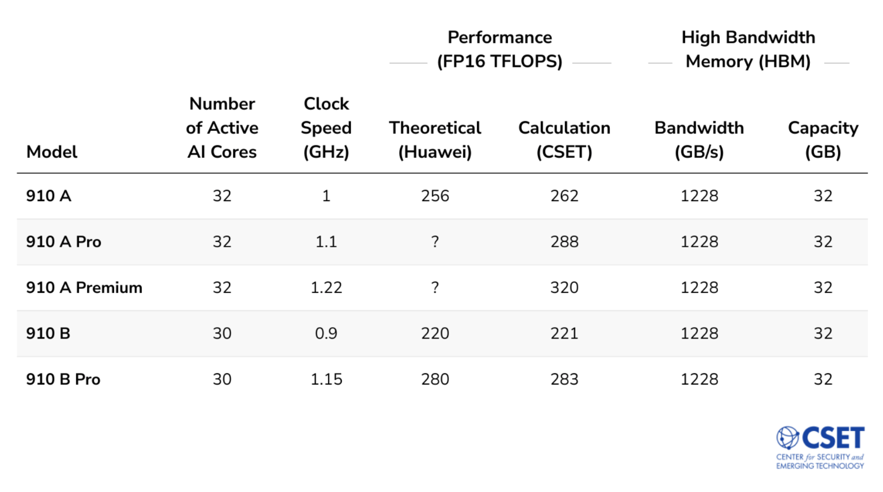
Appendix Table 1: First-Generation Ascend 910 Series (2019) Chip Models14

Note: We were unable to find Huawei-reported performance specifications for the 910 A Pro and 910 A Premium models.
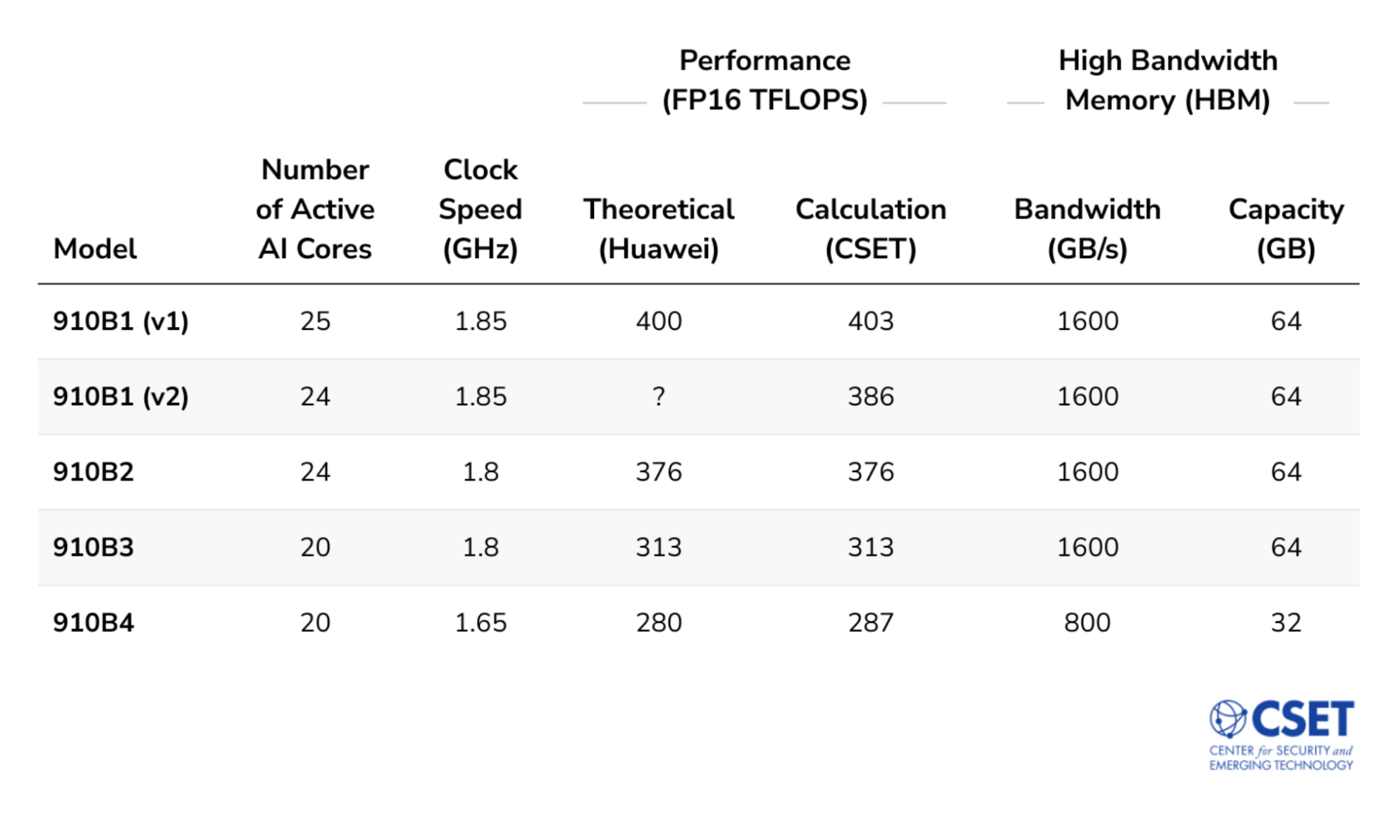
Appendix Table 2: Second-Generation Ascend 910B Series (2022) Chip Models15

Note: We were unable to find Huawei-reported performance specifications for the 910B1 (v2) model.
- The Ascend chips are technically designed by HiSilicon, a wholly owned subsidiary of Huawei. For simplicity, we refer to the designer as Huawei.
- For example, the Zhaohan RA5900-A AI Server (March 24, 2022 version) uses the Ascend 910 A, 910 B, or 910 B Pro. These servers have been used by the Changsha Artificial Intelligence Innovation Center (长沙人工智能创新中心), Chongqing Artificial Intelligence Innovation Center (重庆人工智能创新中心), and Nationwide Integrated Computing Power Network National (Guizhou) Main Hub Center Project (全国一体化算力网络国家(贵州)主枢纽中心项目). Source: https://perma.cc/UB6X-DGRW.
- The 910B series first appeared in documentation in October 2022; however, it is unlikely that the chips were marketed to an external audience before early 2023.
- Note that the nomenclature Huawei uses to describe the first and second generation of its chips is very similar. The first generation chip is called Ascend 910. It has five models, which are named Ascend 910 A, Ascend 910 A Pro, Ascend 910 A Premium, Ascend 910 B, and Ascend 910 B Pro. Huawei’s second generation chip is called Ascend 910B. This version has at least four models, which are named Ascend 910B1, Ascend 910B2, Ascend 910B3, and Ascend 910B4.
- The NVIDIA A100 is capable of 312 FP16 TFLOPS. Source: https://perma.cc/A9VQ-DMK2.
- The IEEE paper detailing the first-generation Ascend 910 architecture explains in detail how the throughput of the vector unit was a key design decision, because the designers wanted to ensure that the vector unit was not a bottleneck for the matrix unit. Source: https://ieeexplore.ieee.org/document/9407221.
- The documentation for the highest-performing 910C chip (i.e., the 910C1) initially specified 50 cores, but in later versions, the core count was reduced to 24 cores, matching the 910B1.
- Sources for first-generation Ascend 910: https://perma.cc/9R9B-3YNA and technical documentation for servers containing Ascend 910 chips. Sources for second-generation Ascend 910B: https://perma.cc/D5XB-DHPH and additional technical documentation. Maximum On-chip Memory: This is the sum of the L0, L1, and L2 cache for the highest performing chip in each series (i.e. 910 A Premium and 910B1). HBM Bandwidth: The first-generation Ascend 910 series has HBM bandwidth of 1228 GB/s across four HBM stacks—307 GB/s per stack; this appears to correspond to the JESD235B specification for HBM2 (https://perma.cc/9FKL-GJDX). The second-generation Ascend 910B series supports HBM2e (https://perma.cc/D5XB-DHPH), also known as JESD235C (https://perma.cc/B3GL-FNTT), which has a maximum bandwidth of 410 GB/s per stack (https://archive.ph/48tV6). In technical documentation, the 910B chips are described as having a maximum HBM bandwidth of 1600 GB/s, which would correspond to 400 GB/s across four HBM stacks. The 910B1, 910B2, and 910B3 each appear to reach this 1600 GB/s maximum with four stacks of 16 GB HBM (64 GB in total per chip). The 910B4, however, appears to only reach 800 GB/s with two stacks of 16 GB HBM (32 GB in total per chip; https://perma.cc/9B7N-X5XT). Fabrication: The second-generation Ascend 910B series is believed to be fabricated on SMIC’s 7nm (N+2) process. See https://perma.cc/2R69-WSBR, https://www.ft.com/content/327414d2-fe13-438e-9767-333cdb94c7e1, and https://archive.ph/RKgTv.
- CSET visualization of maximum theoretical performance for the Ascend 910 and Ascend 910B chips. Specifications for both chips were obtained from technical documentation.
- The IEEE paper detailing the first-generation Ascend 910 architecture specifies that the “three computing units and the MTE work in parallel” (https://ieeexplore.ieee.org/document/9407221). We take this to mean that the operations from the cube, vector, and scalar units can be summed to estimate peak performance. This is supported by a 2019 presentation of the Ascend 910 chip (https://perma.cc/M8NU-YLVQ). Huawei likely excluded the vector unit from the first-generation chips’ performance because the vector units are not accessible at the software level for machine learning calculations. Technical documentation indicates that the vector units are only accessible for the second-generation chips.
- The first-generation Ascend 910 series chip’s 7nm “Vitruvian” compute die measures 31.25mm by 14.6mm (456.25mm2). We do not consider the chip’s “Nimbus” input-output die, because it was fabricated on a mature 16nm process (https://ieeexplore.ieee.org/document/9407221). Vitruvian’s dimensions allow for 120 chips per 300mm wafer (assuming 0.1mm scribe lines and a 3 mm wafer edge exclusion). Each AI core on Vitruvian measures 1.9mm by 3mm (5.7mm2). If, for example, the second-generation Ascend 910B series removed 6 AI cores from Vitruvian (i.e., it only had 26 total AI cores) with no other changes to the area of the die, and if we assume that the removed area only reduces Vitruvian’s longer dimension, the die would measure 28.91mm by 14.6mm (422mm2). In this example, Huawei would be able to fit 131 chips per wafer—a 9 percent increase in the number of chips per wafer from the 910 series to the 910B series. For a Die-Per-Wafer calculator, see: https://anysilicon.com/die-per-wafer-formula-free-calculators/. In reality, this calculation is not as straightforward because Huawei appears to have made other changes to the 910B chip. In each AI core, Huawei added an additional vector unit and decreased the size of the L1 and L0 caches. Huawei also significantly increased the size of the chip-wide L2 cache (from 32 MB to 192 MB). Decreasing the total number of AI cores would help offset the increased size of the L2 cache, preserving some of SMIC’s limited capacity.
- From 2020 to 2024, Nvidia and AMD each released two new generations of AI chips—Nvidia’s H100 and B100 series as well as AMD’s MI250 and MI300 series.
- NVIDIA tripled performance between its A100 (312 FP16 TFLOPS) and H100 (989.5 FP16 TFLOPS) chips. AMD tripled performance between its MI250X (383 FP16 TFLOPS) and MI300X (1307.4 FP16 TFLOPS) chips.
- Sources: https://perma.cc/R6JS-DAHR (list of chip models), technical documentation for servers containing Ascend 910 chips, and additional documentation. The official names of these chips place the letter designation after “pro” or “premium”—e.g. 910 A Pro is really 910 Pro A. We flipped the naming convention for those models to emphasize the relationship among first-generation 910 A models as well as the relationship among first-generation 910 B models. High-Bandwidth Memory: See footnote to Table 1.
- The number of active cores, clock speed, and performance specifications come from technical documentation. For HBM capacity, see 910B1 (https://perma.cc/2UNK-97SX), 910B2 (https://perma.cc/9XX7-6CLD), 910B3 (https://perma.cc/6BSA-EC4P), 910B4 (https://perma.cc/9B7N-X5XT). Two versions of the 910B1: We believe that Huawei reduced the 910B1’s number of active cores from 25 to 24. We labeled the original version of the chip with 25 cores “v1” and the modified, 24-core version as “v2.” Clock Speed (910B3): The clock speed provided by Huawei for the 910B3 was 1.65 GHz. This did not make sense because it indicated that the 910B3 had identical values for the three specifications used to calculate performance (clock speed, core count, and architecture throughput) as the 910B4 but a higher theoretical performance—313 TFLOPS instead of 280 TFLOPS. When we replaced 1.65 GHz with 1.8 GHz (the clock speed for the 910B2), we calculated the expected performance of 313 TFLOPS. Therefore, we believe 1.65 GHz is an error and that the correct clock speed for the 910B3 is 1.8 GHz. Clock Speed (910B4): The clock speed reported for the 910B4 in some technical documentation is 1.5 GHz but in others is 1.65 GHz. The higher value is likely correct because it generates a theoretical performance close to that reported in Huawei’s own documentation. Calculation (CSET): We calculated the performance of each chip using the following equation: (8,704 ops/cycle/core) * (Number of AI Cores) * (Clock Speed in GHz) / 1,000. High-Bandwidth Memory: See footnote to Table 1.
